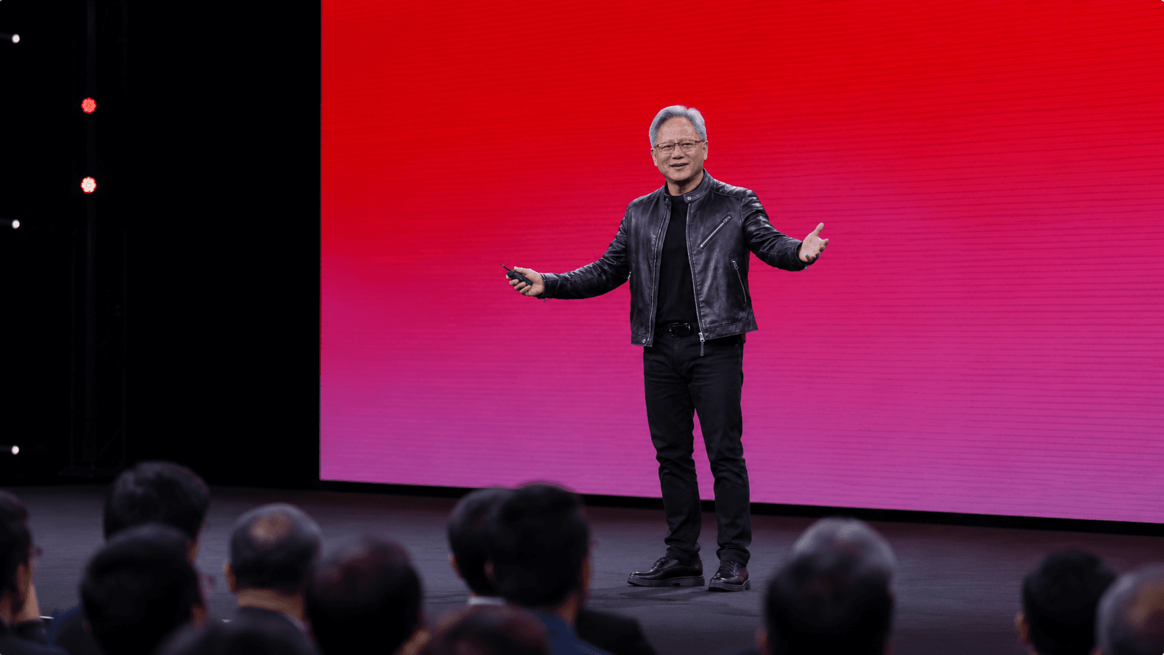
Coherent broke ground today on an expanded manufacturing building in Sherman, Texas, scaling what the company calls the world's first volume 6-inch indium phosphide fab — the production line that feeds NVIDIA's AI networking with lasers, transceivers and pluggable optical modules. Coherent disclosed a $50 million CHIPS Act grant tied to the expansion, building on roughly $17 million in earlier support from the Texas CHIPS program and the Sherman Economic Development Corporation. NVIDIA founder and CEO Jensen Huang attended the ceremony alongside Coherent CEO Jim Anderson, Sherman Mayor Shawn Temann, and Adriana Cruz of Texas Economic Development and Tourism.
The numbers behind the partnership are larger than the grant. In March, NVIDIA committed $2 billion to Coherent to fund R&D and U.S.-based capacity, paired with a multibillion-dollar purchase commitment for advanced laser and optical networking products. That sits inside NVIDIA's broader pledge to produce up to $500 billion of AI infrastructure in the U.S. through industry partnerships, with new sites in Arizona and Texas. Coherent says the Sherman expansion will support more than 550 direct jobs at full capacity, in a city of roughly 45,000 an hour north of Dallas.
The product is unglamorous and load-bearing: indium phosphide wafers that get carved into the lasers and transceivers carrying data between GPUs, racks, and data centers at the speed of light. Compound semiconductors like indium phosphide and gallium arsenide don't get the headlines that logic chips do, but their domestic supply chains have been thin for years — most of the world's InP production still runs on 3- and 4-inch wafers, a generation behind silicon's 12-inch standard.
Key facts
- 01Coherent received a $50M CHIPS Act grant for the Sherman expansion, on top of roughly $17M in earlier Texas CHIPS support.
- 02NVIDIA is investing $2B in Coherent and committed to a multibillion-dollar purchase of laser and optical networking products.
- 03The expanded fab will support more than 550 direct jobs at full capacity in Sherman, Texas, population 45,000.
- 04Moving from 3-inch to 6-inch indium phosphide wafers roughly quadruples usable area per wafer, cutting per-unit cost.
- 05NVIDIA's Vera Rubin Ultra NVL576 links 8 racks of 72 Rubin Ultra GPUs into a single 576-GPU domain, requiring silicon photonics for inter-rack signaling.
Moving to 6-inch wafers roughly quadruples the usable area of a 3-inch wafer, since area scales with the square of the diameter. That translates directly into lower cost per component and the volume the AI buildout requires. Coherent, founded in 1971 as a U.S. manufacturing company, says the Sherman line is the most advanced 6-inch InP fab in the world after 50 years of operation in the materials.
The reason NVIDIA cares is geometry. Its Vera Rubin Ultra NVL576 system links 8 racks of 72 Rubin Ultra GPUs into a single 576-GPU domain over NVLink. At that scale and signaling rate, copper traces can't carry the signal across the distance without burning power on retimers and conditioning. Silicon photonics pays a one-time penalty to convert electrical signals to light, and then distance is nearly free — which is why optics has become the most power-efficient option at NVL576 scale and above.
Coherent's pluggable optics — transceiver modules about the size of a USB stick — plug into the front of NVIDIA networking switches and move data between racks where copper can't reach. The same parts feed NVIDIA Spectrum-X Photonics and Quantum-X Photonics switches with co-packaged optics, where Coherent supplies the external laser module that mounts to the switch's front plate. The roughly two-decade working relationship between the two companies is now structured around keeping optics from becoming the next bottleneck behind compute.
"Coherent is a world-class company, and the work you do is vital to our future, vital to the future of artificial intelligence and vital to reindustrializing the United States," Huang said during a fireside conversation with Anderson at the groundbreaking. The semiconductor laser was demonstrated at room temperature by Bell Labs in 1970, before the technology and most of its manufacturing migrated overseas — a gap the CHIPS Act, funded at roughly $50 billion, was designed to close.
The risks are the usual ones for capital-heavy fabs: yield ramps on a new wafer size are slow and expensive, and demand for AI infrastructure ten years out is a forecast, not a contract. NVIDIA's $500 billion U.S. infrastructure plan and its multibillion-dollar purchase commitment to Coherent reduce that demand risk meaningfully but don't eliminate it. The fab also has to clear environmental and permitting milestones before equipment install begins on the new building.
For NVIDIA, the Coherent expansion is a hedge against the next physical bottleneck in AI scaling. Compute keeps getting denser; the wires between compute don't, which is why optics has moved from a networking line item to a strategic input. Locking in 6-inch InP capacity inside the U.S., on a partner's balance sheet, with CHIPS Act co-funding, is roughly the cheapest way NVIDIA can buy insurance against a future where Rubin-class systems can't be wired together fast enough. The reindustrialization story is real, but the deal logic is supply security.

Working on something we should cover, or seeing a story we missed? Send leads, documents, or feedback to hello@aichatdaily.com. For sensitive tips, see our secure tips page for Signal and PGP options.
Spotted an error? Email hello@aichatdaily.com with the URL and the issue, or read our full corrections policy.